Introduction to NMR/MRI RF Amplifiers
1 INTRODUCTION
Radio Frequency Power Amplifiers (RFPAs) are a vital sub-system of any NMR Spectrometer or MRI scanner. Familiarity with its fundamental function, capabilities and limitations will prove beneficial to the various disciplines of technologists involved with the design, development and use of these machines. The objective is to provide an overview of amplifier technology, terminology, specifications, testing, and evaluation along with future trends in RFPA architectures.
A comprehensive definition of RF pulse parameters is initially provided as the sole purpose of the RFPA is the amplification of the RF pulse. Amplifier specifications are delineated and explained in detail with reference to their impact on the RF pulse sequences. Following the nomenclature, methods of testing and analysis are covered so one can verify performance. A section on application is provided to discuss current and future amplifier architectures, and finally a quick overview of troubleshooting is provided which relates ways in which amplifier performance anomalies can manifest in degradation of system performance.
2 KEYWORDS
Radio Frequency Power Amplifier
Transmitter
Magnetic Resonance Imaging
Nuclear Magnetic Resonance Spectroscopy
3 ABSTRACT
The Radio Frequency Power Amplifier (RFPA) can analogously be thoughtof as the heart of an NMR Spectrometer or MRI Scanner. Although executing a conceptually simple and fundamental task; i.e. making a “small” RF signal into a “big” RF signal, how an RFPA operationally deals with a complex RF Pulse sequence design can have direct impact on Signal to Noise Ratio (SNR) or other parameters with manifestations that are clearly visible in data or MRI scans.
An NMR Spectrometer/MRI Scanner is an extremely complex machine, an understanding of which requires knowledge of Physics, Chemistry, Analog/Digital/Radio Frequency Electronics, Digital Signal Processing etc, etc. One could spend a lifetime on any one of these disciplines relative to NMR/MRI and still fall far short of a total understanding of all there is to know. In addition, a focused expertise on a given individual discipline leaves one lacking in the others. A balanced compromise would be a sufficient working knowledge in several of the areas to gain a solid grasp on the NMR/MRI technology en masse. The objective of this chapter is to provide the NMR/MRI technologist, be they a technician, engineer, scientist, business center manager or radiologist a basic working knowledge of RFPAs such that they understand fundamentally what an RFPA does, what constitutes acceptable current state of the art RFPA performance, how to verify that performance and if it does fall short on expectations, how that shortfall may impact system performance.
4 BACKGROUND
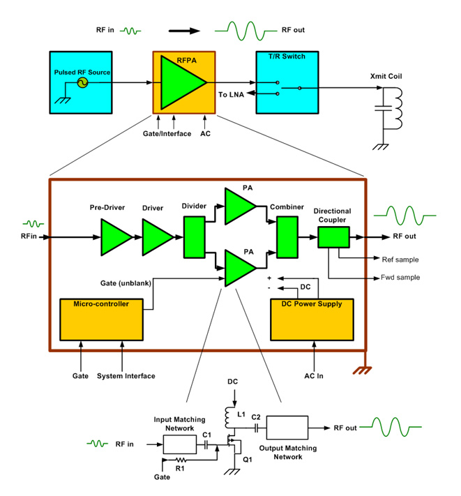 Figure 1.
A system level high level block diagram for an RFPA is shown in Figure #1. The architecture of any NMR/MRI RFPA will generally resemble this block diagram. The function of each block is as follows:
1. The Pre-Driver and Driver are low power amplifier stages that raise the power level of the small, low level input signal up from the milli-Watt range to a level high enough to drive the high power PA sections. Many Power Amplifiers may be required to achieve higher power output levels so divider/combiner networks are deployed to algebraically sum multiple amplifier output power levels together.
2. The Directional Coupler separates out precise, proportional samples of forward and reflected signal power for internal/external power monitoring and fault detection.
3. The DC power supply converts AC line voltages into DC voltages that are suitable to operate the Pre-Driver, Driver, Power Amplifiers and microcontroller.
4. The microcontroller is essentially a micro-computer that continuously runs a fixed program loop that monitors several vital operating parameters throughout the RFPA chassis; DC voltages, currents, pulse width, duty factor, RF output power, load VSWR and temperature. In the event any of these parameters get excessive to a point where damage to the RFPA is imminent, the microcontroller will put the system into a fault mode, shut off appropriate circuits and send out system status via the system interface.
5. The circuit level schematic at the bottom of Figure # 1 shows a basic amplifier stage which consists of input/output matching networks, an active device (Q1), coupling/decoupling components (C1,C2/L1, respectively), DC supply and Gating voltages. This level of circuit breakdown illustrates what is found architecturally in a pre-driver, driver or RFPA amplifier stages. Essentially only two things are done to the RF power that enters into an RFPA: transfer and amplification. Any RF circuit in an RFPA does either one or the other function. In Figure # 1, the input/output matching networks are responsible for matching the system 50 ohm impedance with the low impedances of the RF transistors for maximum power transfer. The coupling/decoupling components (C1, C2 and L1) transfer the RF and DC energy in the appropriate directions. The transistor Q1 amplifies the RF signal.
As stated, the basic function of RFPA is simple; amplify or increase the power of an RF pulse signal applied to its input. If the RFPA was ideal, that is all it would do, the output would be an exact replica of the input waveform, and only the amplitude would be greater by some fixed multiple. But conventional RFPAs are not ideal and they will invariably distort the signal it is meant only to amplify. Just how much it can distort the signal and what is allowable is to be covered.
Since the sole purpose of the NMR/MRI RFPA is to amplify an RF pulse, it’s important to fully understand the parameters that define the ideal RF pulse and also define what RF pulse actually emerges from an RFPA. With that knowledge in mind; it is easier to understand how amplifier performance anomalies degrade the characteristics of the ideal pulse.
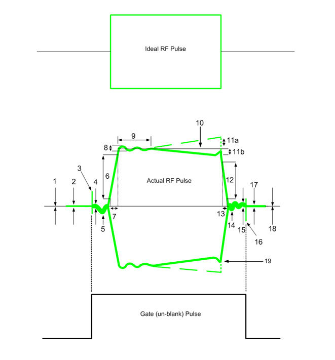
Referring to the ideal pulse in Figure #2, a RF pulse train has several defining parameters, since it is ideal we assume all of them be perfect. Propagating from the baseline on the left, we have a zero volt reference line, continuing to the rising edge of the pulse which goes from zero volts to a fixed amplitude in zero time. The pulse continues exactly at the fixed amplitude until the end of the pulse width duration and again in zero time, the amplitude drops to exactly zero volts.
If we had an ideal RFPA to amplify our ideal RF pulse, the output would look exactly as the input; only the fixed amplitude would be increased by some power amplification factor “A”. But ideal amplifiers do not exist and even the best ones will distort the pulse to some degree.
Observing the RF pulse it after it has exited a non-ideal RFPA. The “actual RF Pulse” in Figure #2 shows an amplifiers output in the Time Domain, and for illustrative and explanatory purposes, most forms of Time Domain pulse distortion that a typical NMR/MRI RFPA can induce are included. It’s interesting to note that while it takes about 4 parameters to define an ideal RF pulse; amplitude, frequency, pulse width and duty factor, it now takes over 17 parameters to characterize a pulse that has been through a non ideal amplifier. Table # 1 defines pulse parameters qualitatively.
5 RFPA SPECIFICATIONS, DEFINITION AND QUANTIFICATION
Any RFPA can be fully specified by quantifying its performance in three domains. A “domain” is simply the “x” axis of a basic “x-y” plot. In the case of RFPAs, “x” will be a “stimulus” that will be varied (i.e., frequency, power etc) while certain “response” parameters (i.e. gain, phase etc) are monitored. The domains necessary to be analyzed to fully characterize a RFPAs RF performance are Time, Frequency and Power domains. The specifications will be conveyed for NMR Spectrometers (NMRS), MRI Scanners (MRIS) and where materially different, EPR (Electron Paramagnetic Resonance) requirements. NQR (Nuclear Quadrupole Resonance) demands are generally satisfied by amplifier specifications that work for MRI requirements, only the operating frequency is usually very low (100kHz-5MHz).
5.1 RFPA specifications, Time Domain
With the RF pulse parameters recently defined, specifying the RFPA in the Time Domain is a natural transition. Please note that all specifications in the Time Domain are in dimensions or ratios of voltages and not power (even though power amplification is the central focus). The reason for specifying in the voltage dimension is more than likely a legacy issue; i.e. “that’s the way it was always done”. One can safely argue that this is the case as power meters that could visually display an Time Domain RF pulse waveform in terms of power dimensions (i.e. Watts or dbm) did not become commercially available until the early 1990’s, which was years after NMR/MRI Time Domain specifications had long been defined and measured by oscilloscopes, which only measure voltage.
5.1.1 Generic Time Domain specifications
Before getting into specific Time Domain requirements, an RFPA for NMR/MRI must meet certain operating pulse requirements. It should be pointed out that an amplifier optimized for pulse operation is vastly different than one that is designed for Continuous Wave (CW) applications. A side by side comparison of a CW and Pulse RF amplifier will reveal the RF circuitry is similar. The primary difference between the two amplifiers is the power supply and heat management technologies. A CW amplifier requires a large DC supply to satisfy the demand for high average power. With high average power comes the need to effectively remove heat, so the heat sinks and fans are substantially larger for a CW RFPA. A pulse RFPA is optimized to provide very high RF power pulses with precise fidelity, but for only short periods of time. The duration of time that a pulse RFPA can put out maximum power is defined as its maximum pulse width. For NMRS, maximum pulse widths are on the order of 300-500 milliseconds, for MRIS, maximum pulse widths are on the order of 20-300 milliseconds. The average power requirements (duty factor) for both NMRS and MRIS are on the order of 10-15% maximum.
5.1.2 Bias enable, disable transient
Transistors in RFPAs are typically fed a DC operating voltage through some type of inductive circuit (See Figure # 1, L1). The purpose of the inductive circuit is to pass DC power to the transistor easily while preventing the amplified RF signal from working its way back into the DC supply. A problem occurs when the bias current is pulsed, the rapidly changing current generates voltage spikes roughly governed by the familiar equation: VL=L (di/dt). This voltage spike can make its way to the output of the RFPA, even if no input RF signal is applied. The duration of this transient is generally very fast and currently has not been shown to inhibit or corrupt images or data; therefore, while it is shown for completeness, it is not formally specified.
5.1.3 Pulse pre-shoot, post-pulse backswing
This distortion occurs directly after an RFPA has been un-blanked (or the RF pulse is terminated) and appears in the time domain as a half or more cycles of a low frequency signal superimposed on the un-blanked noise voltage. It originates in the RFPA output device and is from the bias and operating current energy of the transistors “fly wheeling” (energy being alternatively stored and discharged) between inductive and capacitive decoupling and coupling circuits, respectively (see Fig # 1; L1 and C2). Since it is a very low frequency signal, it will be filtered out by the transmit coil. It is generally not specified because of its ultimate removal by this coil.
5.1.4 Rise, fall time
(Now formally renamed by the IEEE as “transition duration”) “Rise time” is the amount of time an amplifier takes to transition its output at a given power level from 10% to 90% of the voltage waveform. Conversely, “fall time” is the amount of time an amplifier takes to transition its output at a given power level from 90% to 10% of the voltage waveform.
Specification (for both Rise and Fall time): NMRS: <100 nanoseconds, MRIS: 250 nsec to 10 µsec (application dependent), EPR: <25 nanoseconds.
5.1.5 Overshoot, rising/falling edge
This distortion usually occurs from inductively stored energy within the RFPAs circuitry. An RFPA (especially ones used in NMR) has to transition from zero to full power on the order of a 100 nanoseconds, this requires large amounts of current to be switched through inductors very rapidly. This rapid current change causes a voltage spike on the rising and falling edges of the pulse which gets superimposed on the RF pulse.
Specification (for both Rising and Falling edge Overshoot): NMRS: <5%, MRIS: <13%.
5.1.6 Pulse overshoot ringing/decay time
As with the Pulse pre-shoot, energy is being fly wheeled between inductive and capacitive circuits in the RFPA, this effect generates a lower frequency, damped sinusoidal wave that is imposed on initial portion of the RF pulse following the RF rise time and modulates its amplitude. This specification is for the time it takes for the amplitude modulation to drop to less than 5% of the peak RF pulse amplitude.
Specification: NMRS: <500nSec, MRIS: <5 µsec.
5.1.7 Pulse tilt (formerly Pulse droop or amplitude decay)
When an RFPA is pulsed; it is rapidly switched from “off” to “on” states. When the RF transistors in the amplifier are off, they are at certain temperature, when they are turned on, the temperature in the transistor elevates. This increase in temperature can lower (or for certain transistors, raise) the gain of the device over time. If the gain lowers with an increase in temperature, negative tilt (amplitude of RF pulse lowers with increasing time from left to right) occurs. The converse is true for a transistor whose gain increases with increasing temperature, the tilt is now positive, with the amplitude increasing with time.
Specification: NMRS: <5% over 10millisecond rectangular pulse, MRIS: < 8% over a 20 msec rectangular pulse.
5.1.8 Amplitude/Phase Stability, long term
Most of the RF pulse distortion covered to this point addresses a performance deviation local and specific to an individual pulse. Long term amplitude and phase stability is concerned with amplitude and phase characteristics over thousands or millions of pulses during the course of a given pulse sequence. Ideally it is desired to amplify every pulse exactly the same way without any change in amplitude or phase over a period of time which can be minutes or several hours. However, changes in environment, primarily ambient temperature, can alter the relative amplitude and phase of an amplifier as the RF power transistors gain and insertion phase are influenced by temperature.
Specification: Amplitude stability: NMRS, MRIS: <0.2db over 24 hour period, Phase stability: NMRS, MRIS: <3 degrees over a 24 hour period with the ambient temperature being held constant.
5.1.9 Phase error over-pulse
This type of phase distortion occurs across the duration of a rectangular RF pulse. In cases where the Pulse tilt is substantial, the change in output power across the pulse incurs some AM-PM (Amplitude Modulation to Phase Modulation) distortion. This means the phase shift from the input to the output of the amplifier is changing slightly across the time duration of the pulse width.
Specification: NMRS/MRIS: <5 degrees across a 10 msec pulse width
5.1.10 Un-Blanking, Blanking propagation delay time
(Note: there are two types of Un-blanking/blanking delay times, the first is relative to the RFPA and is defined below, the second pertains to the RF pulse sequence and how the un-blank TTL gating signal is timed relative to the RF pulse, the latter is simply the delay time between the median TTL gating transition duration and the immediately following RF pulse transition duration)
To reduce the amount of electrical noise an amplifier emits during the NMR/MRI signal acquisition period, the output stages of an RFPA are shut off by removing bias voltages to the transistors. The objective is to quickly turn the RFPA on, send through some RF pulses, and then quickly turn it off. The signal applied to the RFPA is called a “gating” or “un-blank” signal. It is typically a TTL signal and is synchronous with the RF pulse sequence. It is desired to have the RFPA ready for action as soon as the gating signal is applied. The measure of an amplifiers ability to rapidly turn on and be ready for operation is called “Un-blanking delay” and is measured from the median (50% voltage point) of the gating TTL signal to the median 50% voltage point of the following RF pulse. (Note: the test TTL Gating Signal and the rectangular input RF pulse should have exact, synchronized rise times, assuming the amplifier is TTL active high; TTL High = Amplifier Un-blanked). Conversely, the Blanking delay time is measured from the median of the TTL Gating Fall time to the 50% voltage point of the falling side of the RF pulse (Note: The test TTL gating signals falling transition duration should precede the RF pulses falling transition duration by 100 microseconds so the amplifiers RF output will be truncated by the powering down of the output RF transistors).
Specification: NMRS: 1 µsecond, MRIS: 2µseconds, EPR: 50 nanoseconds
5.2 RFPA specifications, Frequency Domain
This class of specifications cover the RFPAs performance at different frequencies. Ideally, the perfect RFPA would perform exactly the same at one key nuclei frequency as it would at another. The specifications listed below define and quantify certain amplifier parameters such that reasonable uniform performance is achieved at each nuclei.
5.2.1Generic Frequency Domain specifications
The Bandwidth of and RFPA is simply the range of frequencies the amplifier is expected to comply with certain specifications such as output power, linearity, pulse tilt etc. An RFPA can be operated outside of the specified bandwidth, its performance, however, can and will be compromised.
5.2.2 Power Gain
Amplifier Power Gain is simply a measure of how much a particular RFPA will amplify the power of a signal applied to its input. The equation for Power Gain is The way to determine how much Power Gain a RFPA needs for a particular requirement is fairly straightforward, simply take the maximum output power required (Pout) and the maximum input signal power available and substitute the values into the Gain equation. Typically the available input power from most signal sources is on the order of 1 milliwatt or 0dbm. So, for example, if a kilowatt of output power was required, an amplifier with +60 db of Gain is needed.
Specification (NMRS, MRIS): where Pout is required maximum peak power (in Watts)
5.2.3 Gain flatness
The wider the bandwidth a particular amplifier can cover, the harder it is to maintain a constant Power Gain across the bandwidth. It’s more important to have better Gain flatness centered on the key nuclei frequency (+/- 500 kHz) than to try to sustain it over frequencies between nuclei where the amplifier won’t be operated. There is then the need to specify two types of Gain flatness; broadband (or multi-nuclear) gain flatness and nuclei centered gain flatness (where the bandwidth is +/- 500 kHz centered about the key nuclei frequency)
Specification (NMRS, MRIS): Broadband gain flatness: Power Gain (in db) +/- 3db, Nuclei centered gain flatness (+/- 500 kHz): Power Gain (in db) +/- 0.2 db
5.2.3 Harmonic content
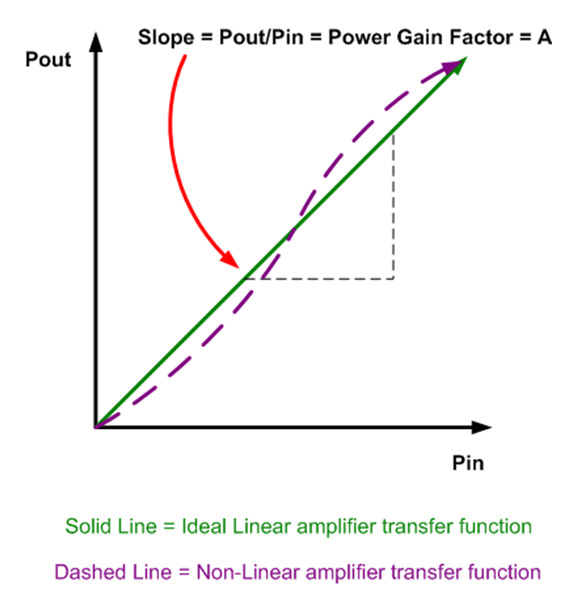
An ideal linear amplifier, if one were to graph its output power versus input power, would have a perfectly straight line (See Figure #3) where the slope of the line would be the Power Gain Amplification Factor. This is simply a number that the input power is multiplied by to solve for the output power. Another characteristic of a linear transfer function is that the output frequency spectrum of the RFPAs output power is simply a larger amplitude replica of the input RF frequency spectrum.
Practical RFPAs are not perfectly linear (the non linearity arising from the non-linear transfer characteristics of the RF power transistors) and the Power Gain Amplification Factor is not a linear multiple but actually a complex transfer function with non-linear terms. Because of the non linear terms, There will be output frequency spectrums not only at in the input frequency spectrum but also at integer multiples (2, 3, 4…n) of the input frequency. This is known formally as Harmonic Distortion or Harmonic Content. The bulk of the harmonic energy will be filtered out by the transmit coil, so low pass filtering of the RFPAs output is usually not required.
Specification (NMRS, MRIS): even order harmonics: -20 dbc, odd order harmonics: -12 dbc
5.2.4 Spurious RF output emissions (oscillation)
There are many forms of amplifier stability. Amplitude stability, for example, is a measure of the amplifiers ability to maintain a constant output level over long pulse sequence durations. A generic form of amplifier stability is its ability to maintain an output that is in some way controlled by the input. Spurious RF outputs are erratic frequency components that an RFPA puts out that can be either in its operational bandwidth or outside. The spurious output sometimes caused by inadequate filtering of output DC feed lines that couple RF signal power from the output of the RFPA to the input. They can be initially generated when an RF input is applied, yet can remain when the RF input is shut off. They are generally non harmonic related and can be close in or far away in frequency from the carrier. Wherever they are located, however, they are referenced in amplitude to the carrier frequency.
Specification (NMRS, MRIS) : < -50dbc
Another type of amplifier stability is “Load-Pull” stability. This is a measure of the amplifiers ability to maintain stable (or spurious-free spectral) operation while the output (or input) is subjected to various load impedances. Historically, amplifiers have been unrealistically specified as “unconditionally stable” for any magnitude/phase of source/load impedance.
The problem with an “unconditionally stable” requirement is that there is an infinite amount of source and load combinations to apply to an amplifiers terminals. In practicality, this simply cannot be verified.
In reality, the only true “unconditionally stable” two port network is a passive (Gain<1) network.
A more realistic way to specify and be able to verify amplifier stability is to define a load space on the Smith Chart and pick load Reflection Coefficients with discrete magnitude and phase values on which to test for spurious response.
For example, a specification for amplifier stability may read: Conditionally stable for up to 3:1 load VSWRs, rotational about the Smith Chart at 45 degree increments with less than -50 dbc of spurious frequency components.
5.2.5 Input VSWR (Input Return Loss)
Input Voltage Standing Wave Ratio or Input VSWR is measure of how close the input impedance of the amplifier is to an ideal 50 ohm resistor. The closer it is, the better it is matched to the RF signal source (assuming it has a 50 ohm output) and the better this match is, the more power will transfer from the pulse signal source to the RF amplifier. A 1:1 VSWR is a perfect match (i.e. all the power from the RF signal source will enter the RF amplifier). The higher the first number goes, the worse the impedance match is, and subsequently less power enters the RFPAs input.
Return loss is simply another way to express input match, only this is expressed as a logarithmic ratio of forward and reflected power.
Specification (NMRS, MRIS): Input VSWR: <2.0:1, Input Return Loss : <-9.5db
5.2.6 Output Noise (Blanked)
The NMR signal, be it from a patient or a sample is very faint. One way to improve Signal to Noise ratio is reduce all unnecessary electrical noise from the environment where the NMR signal is present. An RFPA generates quite a bit of noise while it is on as it has a large amount of Gain. The best way to reduce electrical noise out of an RFPA would be to simply shut it off. The problem with that is it takes far too long to turn the entire amplifier system on and off for it to be effectively used in an NMR/MRI system. The next best thing is only shut off the final stages of power amplification. This is accomplished by shutting off the bias to the output transistors as they can be switched on/off in under a microsecond. There will still be some noise output even with the output stage blanked off, to be certain, but the noise output now is tolerable.
Specification (NMRS, MRIS): -20db over thermal noise.
5.2.7 Noise Figure
A RFPAs job is to transmit sometimes very large amounts of RF power into a sample or patient. The magnitude of this RF energy is very large in comparison to the NMR signal. It may not seem essential for an RFPA to have a low noise output while it is transmitting since the very thing it is tasked to do is to generate RF power and lots of it. Why then would noise figure be important? The reason is that there are applications where the RFPA is transmitting at one frequency, however the RF receivers are listening at another and the lower Noise Figure an RFPA has, the less it will interfere with this second frequency.
Specification (NMRS, MRIS): <10 db
5.3 RFPA specifications, Power Domain
This is the last of the three Domains. In this area of specifications, the stimulus to be varied is power, that is, the input power to the RFPA is swept across a certain dynamic range (range of power levels, usually 30-40db). For example, if an RFPA is driven to full power at 0 dbm input, this unit would be tested with an input RF power level of -40 to 0 dbm. While the power is being varied, certain response parameters are being recorded such as Gain and Phase Linearity.
5.3.1 RF Power output
An RF Power Amplifiers output power capability is by far the first and foremost parameter that comes to mind when discussing an RFPA. How much power to use for a particular application in an NMR Spectrometer or MRI Scanner depends on many, many factors: coil (probe) limitations, SAR values, part of the anatomy to be scanned (i.e. head, extremities, and whole body) etc. It is truly beyond the scope of this discussion to quantitatively convey how to specify a maximum power output level for all applications. What can be discussed, however, is a rough estimate of what has been typically used to date. NMR RFPAs usually deposit their outputs into to some chemical sample, the size of the sample generally not large in volume. Most NMR applications run less than 500-2 kW of peak power up to 400MHz, from 400 MHz to 1 GHz, 100-500 Watts is adequate and from 1-2 GHz, 30-100 Watt amplifiers have been deployed.
MRIS RF power requirements can vary widely, as discussed. For extremities (arms, legs) in the 1- 3T realm 500-2kW is common, for head imaging, 4-8kW, and whole body amplifiers with up to 35 kW have been used. For higher fields (4, 7, 8, 9.4, 10.5 and eventually 11.7T) requests for power levels of up to 10-20kW are common. Multichannel 3T systems are running at 4kW per channel and multichannel 7T RFPAs are designed for 1kW per channel.
NQR applications have operated in the 2-4kW range and the far less common EPR experiments have be executed with anywhere from 400-2kW.
Although NMR and MRIS RFPAs are primarily used for pulsed applications, they are certain applications where they can be required to run in Continuous Wave (CW) mode. In this event, the required CW power is usually no more than 10% of the amplifiers maximum peak RF output power.
5.3.2 Gain Linearity
Pulse sequences can contain RF waveforms that have precisely proportioned amplitude ratios. An ideal linear amplifier has the unique characteristic that its output power is linearly proportional to the input power. Figure # 3 shows this graphically, which is a plot of output power vs. input power. The linear trace is called a transfer function, which describes the transfer relationship of input to output power of an amplifier.
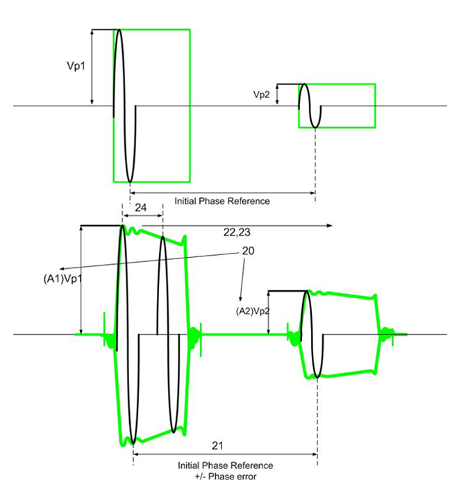
The slope of the line is the power gain factor “A”, which (in an ideally linear amplifier; solid, straight plot) is some fixed, constant number regardless of what power level the output is. In actuality, the transfer function will not have a slope with a constant power gain factor, but one that is not linearly proportional to the input and will change over the dynamic range of the amplifier (dashed, curved plot). What this translates to is an amplifier that will amplify signals at low power one way, medium power another way and high power yet another way. By different “ways” of amplification, it is meant that different power levels will be amplified by different power gain factors. This translates to a non linear gain transfer function. Figure # 4 shows how different amplitude pulses get different Power Gain Factors (A1 and A2).The Gain linearity specification quantifies how much deviation from ideal linear operation an actual amplifier can deviate from. In cases where the deviation from ideal is severe, the carefully proportioned amplitude ratios in a given pulse sequence can change dramatically.
The Gain linearity specification comes with a definition of dynamic range requirement as it must be understood and clarified, a priori, where the amplifier will be expected to be operated in terms of output power level. Usually the dynamic range is taken from the maximum specified output power level to some amount of db down from this level. The amount of dynamic range defined as a minimum should be 20 db, typically 40 db and in extreme performance applications 60 db.
Specification (NMRS, MRIS): Gain Linearity over 40 db dynamic range: +/- 1db of gain variation.
5.3.3 Phase Linearity
It takes a finite amount of time for a signal to make its way through an RFPA from its input connector to its output, and although it makes it through very fast (on the order of nanoseconds) there is a definite time expended. This delay time is called propagation delay and integral with this measurement is the parameter Insertion Phase. This is a measure of relative phase shift from the input to the output of the RFPA. As with Gain Linearity, it would be preferred to have this relative phase shift to remain constant across the defined dynamic range of the RFPA. If the phase shift was constant then relative phase relationships between low power pulse signals and high power ones would be preserved throughout the amplification process. If the relative phase shift changes over the dynamic range, then the phase relationships are altered. This deviation is defined as Phase Linearity, and as with Gain Linearity, if comes paired with a defined dynamic range. The root cause of phase non-linearity is a parasitic junction capacitance present in all types of RF power transistors. This capacitance varies as a function of output power, so as the output power changes, so does this capacitance and along with it, the relative phase shift through the RFPA.
Specification (NMRS): Phase Linearity over 40 db dynamic range: +/- 5 degrees of insertion phase variation. Phase Linearity (MRIS): +/-7.5 degrees of insertion phase variation.
5.4 Safety specifications and System compatibility considerations (IEC-60601 and CE mark)
Up to this point, the primary focus has been the amplifiers performance relative to its ability to accurately reproduce an RF pulse sequence with an acceptable degree of fidelity. There are two other broad areas of amplifier specifications that worth covering in general so the end user or system engineer can be informed of their implications.
Safety is of primary importance with any electrical device, and RFPAs are certainly no exception. Specific Absorption Rate (SAR) is concerned with how much average RF power is deposited into a patient, one should be very clear on what the limitations are and have appropriate protection and limiting devices in place to automatically shut the RF amplifier off in the event SAR guidelines are exceeded. It is strongly recommended to have operationally redundant protection measures (i.e. independent, simultaneously operating average RF power monitoring devices) to limit RF power.
In addition to safety relative to the patient, safety concerns relative to the individuals who work with the RF power amplifier hardware are equally as important.
The safety protocol for both SAR and medical equipment is covered under the IEC-60601 safety standard. From the equipment perspective, an RFPA compliant to IEC-60601 will have undergone several months of independent safety tests performed on the unit. Organizations such as Underwriters Laboratories (UL) conduct thorough safety tests (including, but certainly not limited to) that verify the outer chassis is adequately grounded, wire insulation is appropriate for the voltage on a given conductor, circuit breakers and fuses are properly rated for deployment and that various, single point circuit failures will not present a hazard to the user. Perhaps most important, a unit that is marked as a “UL recognized component”, throughout the duration of that RFPAs manufacturing life cycle, the manufacturer will be subject to random audits to confirm the product is made conformant to the original UL approved design in terms of materials, components and also that the appropriate UL mandated production safety verification tests are conducted with test equipment that is calibrated and within its specified calibration cycle.
System Electro-Magnetic Compatibility (EMC) is covered by the CE Mark. The CE Mark is what the manufacturer applies to an RFPA after the unit has undergone and passed a battery of EMC tests. EMC tests are concerned with two major attributes of the RFPA; emissions and susceptibility. RFPAs generate a large amount of RF energy, the emissions aspect of EMC/CE testing measures the RFPAs ability to limit and contain its own radiated (RF energy emitted out of the RFPA chassis into its environment) and conducted (RF energy exiting the RFPA on interface and AC power cables connected to the unit) energy. This is a rough measure of how much a RFPAs operation may affect adjacent equipment.
The susceptibility portion of EMC/CE testing attempts to measure a RFPAs vulnerability to radiated (RF energy it receives from other equipment through the air) and conducted (RF energy it receives internally conducted through AC power lines and interface cables) energy.
In summary, the CE mark/EMC testing is a measure (however, by no means a guarantee) of how well an RFPA might perform in a given system environment. A unit that has a CE mark should be less likely to interfere with other equipments and conversely, its operation should be less impaired by other co-located noise generating electrical device, environmental disturbances (such as Electrostatic Discharge, ESD), lightning and AC power line surges and dips.
5.5 RFPA amplifier classes
RFPAs are designed to run in certain “classes” of operation. A class of operation loosely defines how the transistors in an RFPA amplify an RF pulse signal. Transistors operating in Class A amplify the full 360 degrees of the RF sinusoidal signal. Class A amplifiers are the most linear, most rugged (ability to tolerate bad loads), least efficient (<20%) and most expensive class of amplifier operation. Transistors operating in Class AB amplify slightly more than 180 degrees of the RF sinusoidal signal. Class AB offer a tradeoff of acceptable linearity reduced ruggedness, improved efficiency (approx 50%) and cost effectiveness. Class D/E amplifiers operate in switch mode (the transistors are switched on/off at the input RF frequency) are highly efficient (approximately 70%), yet extremely non-linear and require complex linearity error correction networks to make them usable for MRI.
6.0 RFPA TESTING AND EVALUATION
The goal of this section is to provide the technologist with quick, cost effective and most of all easy way to test and evaluate an RFPAs performance. It is not intended to cover comprehensive test procedures, rather brief, discrete tests that use test equipment found in most NMR/MRI facilities and, if properly executed, can reasonably verify if an RFPA is functional within certain specification.
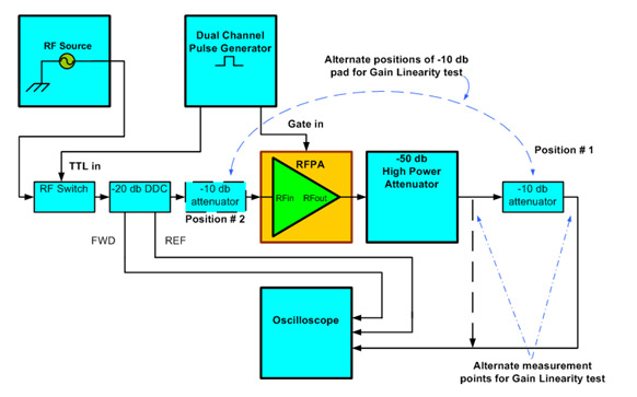
Figure # 5 shows only one required test equipment configuration and very few pieces of equipment needed for measurement. The other necessary test equipment is as follows (remember to be certain to use only equipment that is within its recommended calibration cycle):
A RF signal source; capable of covering the entire frequency range of the RFPA, and with at least 10 dbm (10 milli-watts) output capability of stable, clean, spurious and harmonic free sinusoidal signal.
- A dual channel pulse generator, with TTL output levels and the ability to synchronize its two pulse outputs, yet independently vary the pulse width and duty factor of each channel.
- A 4 channel, digital storage oscilloscope, with a frequency capability well in excess (at least 2 times) the maximum frequency of the RFPAs upper limit.
- A high speed RF Switch with switching speed on the order of 5 nanoseconds and one that will switch the CW RF output from the RF source producing a waveform that approaches an ideal RF pulse as closely as possible; i.e.: fast rise/fall times, zero overshoot, ringing and pulse tilt.
- A Dual, Directional Coupler (DDC) with a coupling value of -20db, directivity of better than -20 db and insertion loss less than -0.75 db across the operating bandwidth of the RFPA. Be certain to obtain exact coupling values vs. key nuclei frequencies.
- Two attenuators, one a -50db high power attenuator that can handle both the peak and average RF power output of the RFPA under test. A second, lower power -10 db power attenuator that can handle the RFPAs peak and average RF power output of the RFPA after -50 db of output signal attenuation. Be certain that both attenuators operate over the bandwidth of the RFPA under evaluation. Obtain the exact attenuation values at key nuclei frequencies either from the manufacturer using the method described using the oscilloscope.
- All required RF test cables, connectors and adapters capable of handling the peak and average RF power levels from the RFPAs output.
6.1 Useful equations and conversions
For simplicity, the tests have been designed such that only one measurement device, the digital oscilloscope (aka “scope”), is required. A scope only measures voltages, so for tests where it is needed to know what the power level is; conversion from volts to watts is required. Equations to do this conversion are presented along with ways to convert and work with power in dbm (power referenced to 1 milliwatt) as this will make calculations significantly easier.
A simple sine wave is shown in Figure # 4, the scope measures it in the Time Domain as a peak to peak voltage and is denoted as 2 (vp1). To convert this measured voltage to power, we first must convert the peak to peak voltage to an RMS value: vrms = (vp1) (0.707). For all the tests, the input impedance of all devices must be 50 ohms. With that in mind, the power measured of the sinusoidal waveform of Fig. # 4 Pmeasured = (vrms)2/50. Finally, as you will see shortly, if this number is converted to dbm with the following equation: , many calculations will be simplified.
With all this in mind, proceed as follows:
- Set the RF Source to the lowest operating frequency (Flow) of the RFPA
- Set Pulse generator to have a pulse width of 1 msec and 10% duty factor on the channel feeding the TTL control on the RF switch, set the channel feeding the Gate input to the RFPA to un-blank 10µsec before the RF pulse is turned on and to blank 10 µsec after the RF pulse is turned off.
- Using the oscilloscope, apply +10 dbm to the input of the DDC and measure the voltage at the Forward (FWD) port. Convert this to dbm and subtract from 10dbm, this is the exact coupling value (truncate coupling value beyond the tenth of a db). Repeat for the Reflected (REF) port. Enter this value in the appropriate row/column in Table # 2
- Using the oscilloscope, apply +10dbm to the input of the -50db pad and measure the voltage at the output port. Convert this to dbm and subtract from 10, this is the exact attenuation value. Repeat for the Reflected -10db pad. Enter these values in the appropriate rows/columns in Table # 2
- To solve for the peak to peak voltage to be measured on the oscilloscope (that is measuring voltage on the output of the 50 and 10 db attenuator) which would correspond to a full power reading, convert the full power in watts to dbm, subtract the actual, measured high power attenuators attenuation value in db from this value. Then convert the remaining number from dbm to watts, then from watts to peak to peak voltage.
For example, given a 1kW amplifier:
Pout (max) = 1kW = 60 dbm
60 dbm - 60 db (from 50 and 10 db attenuators) = 0dbm = 0.633 volts peak to peak
- Connect the equipment as shown in figure # 5, and increase the drive output of the RF source until the full output power of the amplifier is reached (i.e. the voltage from the calculation in step # 5 is seen on the oscilloscope)
- Use the scope to fully measure and characterize the pulse performance in terms of rise- time, overshoot, tilt and fall-time. Enter these values in the appropriate rows/columns in Table # 2
- Measure the peak to peak voltage at the DDC FWD and REF ports. Convert these values to dbm. Enter these values in the appropriate rows/columns in Table # 2. Remember the voltages measured by the oscilloscope are scaled down voltages whose magnitude was reduced by the DDC and output attenuator. To get the actual voltages at the terminals of the RFPA, remember to covert the voltage read by the oscilloscope to power (in dbm), then add the respective attenuation or DDC coupling values to this power to get the actual power at the input/output ports of the RFPA.
- Move -10db pad to input of the RFPA, measure the voltage at the output of the -50 db attenuator, convert to dbm and subtract from power level measured previously out of -10 db pad. Enter this value in the appropriate row/column in Table # 2
- Once all the values are entered, you can now know what the rise/fall-times, overshoot, ringing and tilt values and can calculate output power, gain, single point gain linearity (either compressive or expansive) and input Return Loss
- Repeat the process over the low, mid and high frequencies of the RFPAs bandwidth or simply at key nuclei frequencies.
Upon completing the tests and the associated calculations, the data can be compared with the published RFPAs specifications. Bear in mind that the test technique presented will yield fairly good results but may vary from the manufacturer’s data due to difference in test technique and measurement unCertainty.
7 RFPA SYSTEM INTEGRATION
With the performance of the RFPA verified, it’s time to integrate the RFPA into the system. A few topics are worth mentioning when installing an RFPA:
- Rack-mounting: Most RFPAs come in a standard 19 inch rack mountable package. A rack without front/rear doors is preferable (but not mandatory) from an air flow perspective. Mount the RFPA on the lowest spot available for a low center of gravity and a stable rack. If you are to make one and only connection properly, be certain to adequately ground the RFPA chassis to the rack ground (using 6 gauge green/yellow band wire) and the ground the rack to the system ground.
- Location: The amplifier should be as close to the coil as possible to minimize cable losses (especially at high fields such as 7T). Most RFPAs can work in fringe fields of 50 gauss, so a balance would be as close to the coil without materially exceeding this level of fringe field.
- RF Connectors: A few quick words on connectors. First, there is no magic number for maximum peak/average power handling capability; several factors weigh in; operating frequency range, load mismatch, ambient temperature, altitude and manufacturer. What’s listed here is fairly conservative. You only need to be familiar with the following connectors: BNC: good for RF input (0 dbm power levels) cables and gating signals, that’s it. The following connector power ratings apply up to 2GHz: SMA: Can be used up to 1kW peak, 100W average power, Type N: 10kW peak, 500 W average power. Type SC: 50kW peak, 2kW average power .Type 7/16th: 13 kW peak, 3kW average.
- RF Coaxial Cables: There are literally dozens of RF coaxial cable types. The primary parameters to bear in mind when selecting an RF Cable are: Insertion Loss (in db per foot), Peak/Average power handling capability, flexibility (if you intend to move it frequently) and cost. And speaking of cost, especially at high fields (4, 7, 9.4T etc), the RF cable is not an item to cut corners on. An RFPA for 9.4T may cost $50-$100,000.00. A coax cable run with poor loss characteristics of -3db can cost you $25-$50,000.00 in RF power! A few recommendations are Times Microwave LMR-400, Andrew heliax and HF Electronics Ecoflex.
- Protection: Coil research can be a trial and error process in which the RFPA can be subjected to extreme load VSWRs that can be detrimental. Poor load VSWRs can send large amounts of reflected power back at the output of the RFPA and may damage its transistors. Electronic protection (i.e. VSWR fault circuitry) can shut the amplifier down in the event excessive reflected power is detected, however VSWR fault circuits engage on the order of microseconds and some RFPA damage can occur in this time duration. The most effective RFPA protection involves the installation of circulators in line with the output. Any reflected RF power will be instantaneously diverted to a high power RF isolation load. The main drawbacks with circulators are they are narrowband, lossy and only available at frequencies down to about 120MHz.
8 RFPA SYSTEM APPLICATIONS; CURRENT AND FUTURE
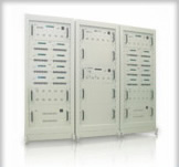
The NMR/MRIS RFPA architecture has changed little in the past 20-25 years. Tube amplifiers currently represent a fairly cost effective modality for narrowband proton amplifiers in 1.5T and 3T. These are slowly being supplanted by solid state equivalents. At field strengths of 3T and higher, obtaining a uniform B1 field presents a substantial challenge. To alleviate this issue, multi channel RF amplifiers (typically anywhere from 8-16 amplifier channels) have been deployed for B1 shimming. The amplifier requirements and specifications do not vary much, only now the individual amplifier channels need to matched for Insertion Gain and Phase. Matrixed amplifiers (amplifiers that can switch between multichannel mode and combined amplifier mode) are now being used where there is a desire to use the RFPA in a conventional single output or switch to a multi-channel output mode. The primary challenges in multi channel (B1 shimming) RFPAs are the gain/phase matching of up to 16 independent channels, especially if the amplifiers are broadband. Another issue is the coupling between transmitter elements which can lead to high levels of reflected power into the RFPAs output and virtual VSWR fault triggering(i.e. reflected power that is not from an adverse load but from element to element coupled power)
There is an ongoing move to develop amplifiers that can be located either in the bore (high field compatible) or mounted just outside the bore. High efficiency amplifiers may find use as they run nearly twice as efficient as conventional Class AB amplifiers which may make them a suitable candidate for “in-field” RFPAs.
9 TROUBLESHOOTING MATRIX
Table #3 provides a brief matrix which list several types of amplifier performance anomalies and links them with possible manifestations of system performance degradation. Note that these are only possible causes that can be RFPA related, there may be other sub-system problems that can also cause similar issues.
Ref. |
Parameter name |
Description |
Dimension |
1,18 |
Ideal, zero volts reference line |
Mathematical construct, point of reference for all pulse voltages |
volts |
2,17 |
Blanked noise voltage |
Noise voltage out of RFPA when blanked |
volts |
3 |
Bias enable transient voltage |
Voltage spike exiting RFPA when RFPA is initially un-blanked pre-RF pulse |
volts |
4,15 |
Un-blanked noise voltage |
Noise voltage out of RFPA when un-blanked |
volts |
5 |
Pulse pre-shoot |
Amplifier output zero volt reference deviation prior to pulse rise |
% |
6 |
Pulse rising edge |
10-90% voltage transition range |
volts |
7 |
Pulse rise transition duration |
Time required for amplifier to transition from 10-90% of peak output voltage |
micro/nano-seconds |
8 |
Rising pulse overshoot |
Portion of RF pulse that exceeds 100% amplitude during post rising transition duration |
% |
9 |
Pulse overshoot ringing/decay time |
Time for damped sinusoidal envelope peak to decay |
micro/nano-seconds |
10 |
100% pulse RF amplitude reference |
Point on RF pulse that is chosen to be 100%, usually after overshoot and ringing are done |
volts |
11a,b |
Pulse tilt positive/negative |
Amount that peak RF voltage slopes throughout pulse width duration |
% |
12 |
Pulse falling edge |
90-10% voltage transition range |
volts |
13 |
Pulse falling transition duration |
Time required for amplifier to transition from 90-10% of peak output voltage |
micro/nano-seconds |
14 |
Post pulse backswing |
Amplifier output zero volt reference deviation after pulse fall time |
% |
16 |
Bias disable transient |
Voltage spike exiting RFPA when RFPA is blanked post-RF pulse |
volts |
19 |
Falling pulse overshoot |
Portion of RF pulse that exceeds final tilt amplitude pre-falling transition duration |
% |
20 |
AM-AM distortion |
Inter-pulse amplitude ratio distortion, also known as gain linearity |
db |
21 |
AM-PM distortion |
Inter-pulse relative phase distortion, also known as phase linearity |
degrees |
22 |
Amplitude stability |
Long term gain stability over time |
db/hours |
23 |
Phase stability |
Long term phase stability over time |
degrees/hours |
24 |
Phase-error, over-pulse |
Phase shift across the duration of a pulse width |
degrees |
Table # 1 Pulse Parameter Definitions
|
Measurement |
Dimension |
F(low) |
F(mid) |
F(high) |
1. Forward coupling (measured) |
db |
|
|
|
2. Reflected coupling (measured) |
db |
|
|
|
3. -50 db atten. (measured) |
db |
|
|
|
4. -10 db atten. (measured) |
db |
|
|
|
5. Test power output |
dbm |
|
|
|
6. Vp-p at -10db attenuator output |
volts |
|
|
|
7. Rising transition duration |
nsec |
|
|
|
8. Falling transition duration |
nsec |
|
|
|
9. Pulse overshoot |
% |
|
|
|
10. Pulse tilt |
% |
|
|
|
11. Input forward power |
dbm |
|
|
|
12. Input reflected power |
dbm |
|
|
|
13. Input return loss=(11-12) |
db |
|
|
|
14. Gain= (5-11) |
db |
|
|
|
15. QPower (-10 db pad @position#1) |
dbm |
|
|
|
16. Power (-10db pad @position#2) |
dbm |
|
|
|
17. Gain compression/expansion (15-16) |
db |
|
|
|
Table # 2 Amplifier Test Data
|
Amplifier performance anomaly |
Symptom |
Excessive gain non-linearity |
Slice profile distortion |
Excessive phase non-linearity |
Slice profile distortion |
Excessive pulse tilt |
Slice profile distortion |
Excessive pulse overshoot |
Slice profile distortion |
Excessive rising/falling transition duration |
Slice profile distortion |
Excessive blanked noise output |
Low signal to noise ratio, noisy image |
Gain instability |
Image ghosting/shading |
Phase instability |
Image ghosting |
Spurious oscillation |
Image artifacts/streaking |
Low power output |
Inability to achieve desired flip angles, increased spatial distortion |