Amplifier Tutorials

5 RFPA SPECIFICATIONS, DEFINITION AND QUANTIFICATION
Any RFPA can be fully specified by quantifying its performance in three domains. A domain is simply the x axis of a basic x-y plot. In the case of RFPAs, x will be a stimulus that will be varied (i.e., frequency, power etc) while certain response parameters (i.e. gain, phase etc) are monitored. The domains necessary to be analyzed to fully characterize a RFPAs RF performance are Time, Frequency and Power domains. The specifications will be conveyed for NMR Spectrometers (NMRS), MRI Scanners (MRIS) and where materially different, EPR (Electron Paramagnetic Resonance) requirements. NQR (Nuclear Quadrupole Resonance) demands are generally satisfied by amplifier specifications that work for MRI requirements, only the operating frequency is usually very low (100kHz-5MHz).
5.1 RFPA specifications, Time Domain
With the RF pulse parameters recently defined, specifying the RFPA in the Time Domain is a natural transition. Please note that all specifications in the Time Domain are in dimensions or ratios of voltages and not power (even though power amplification is the central focus). The reason for specifying in the voltage dimension is more than likely a legacy issue; i.e. thats the way it was always done. One can safely argue that this is the case as power meters that could visually display an Time Domain RF pulse waveform in terms of power dimensions (i.e. Watts or dbm) did not become commercially available until the early 1990s, which was years after NMR/MRI Time Domain specifications had long been defined and measured by oscilloscopes, which only measure voltage.
5.1.1 Generic Time Domain specifications
Before getting into specific Time Domain requirements, an RFPA for NMR/MRI must meet certain operating pulse requirements. It should be pointed out that an amplifier optimized for pulse operation is vastly different than one that is designed for Continuous Wave (CW) applications. A side by side comparison of a CW and Pulse RF amplifier will reveal the RF circuitry is similar. The primary difference between the two amplifiers is the power supply and heat management technologies. A CW amplifier requires a large DC supply to satisfy the demand for high average power. With high average power comes the need to effectively remove heat, so the heat sinks and fans are substantially larger for a CW RFPA. A pulse RFPA is optimized to provide very high RF power pulses with precise fidelity, but for only short periods of time. The duration of time that a pulse RFPA can put out maximum power is defined as its maximum pulse width. For NMRS, maximum pulse widths are on the order of 300-500 milliseconds, for MRIS, maximum pulse widths are on the order of 20-300 milliseconds. The average power requirements (duty factor) for both NMRS and MRIS are on the order of 10-15% maximum.
5.1.2 Bias enable, disable transient
Transistors in RFPAs are typically fed a DC operating voltage through some type of inductive circuit (See Figure # 1, L1). The purpose of the inductive circuit is to pass DC power to the transistor easily while preventing the amplified RF signal from working its way back into the DC supply. A problem occurs when the bias current is pulsed, the rapidly changing current generates voltage spikes roughly governed by the familiar equation: VL=L (di/dt). This voltage spike can make its way to the output of the RFPA, even if no input RF signal is applied. The duration of this transient is generally very fast and currently has not been shown to inhibit or corrupt images or data; therefore, while it is shown for completeness, it is not formally specified.
5.1.3 Pulse pre-shoot, post-pulse backswing
This distortion occurs directly after an RFPA has been un-blanked (or the RF pulse is terminated) and appears in the time domain as a half or more cycles of a low frequency signal superimposed on the un-blanked noise voltage. It originates in the RFPA output device and is from the bias and operating current energy of the transistors fly wheeling (energy being alternatively stored and discharged) between inductive and capacitive decoupling and coupling circuits, respectively (see Fig # 1; L1 and C2). Since it is a very low frequency signal, it will be filtered out by the transmit coil. It is generally not specified because of its ultimate removal by this coil.
5.1.4 Rise, fall time
(Now formally renamed by the IEEE as transition duration) Rise time is the amount of time an amplifier takes to transition its output at a given power level from 10% to 90% of the voltage waveform. Conversely, fall time is the amount of time an amplifier takes to transition its output at a given power level from 90% to 10% of the voltage waveform.
Specification (for both Rise and Fall time): NMRS: <100 nanoseconds, MRIS: 250 nsec to 10 sec (application dependent), EPR: <25 nanoseconds.
5.1.5 Overshoot, rising/falling edge
This distortion usually occurs from inductively stored energy within the RFPAs circuitry. An RFPA (especially ones used in NMR) has to transition from zero to full power on the order of a 100 nanoseconds, this requires large amounts of current to be switched through inductors very rapidly. This rapid current change causes a voltage spike on the rising and falling edges of the pulse which gets superimposed on the RF pulse.
Specification (for both Rising and Falling edge Overshoot): NMRS: <5%, MRIS: <13%.
5.1.6 Pulse overshoot ringing/decay time
As with the Pulse pre-shoot, energy is being fly wheeled between inductive and capacitive circuits in the RFPA, this effect generates a lower frequency, damped sinusoidal wave that is imposed on initial portion of the RF pulse following the RF rise time and modulates its amplitude. This specification is for the time it takes for the amplitude modulation to drop to less than 5% of the peak RF pulse amplitude.
Specification: NMRS: <500nSec, MRIS: <5 sec.
5.1.7 Pulse tilt (formerly Pulse droop or amplitude decay)
When an RFPA is pulsed; it is rapidly switched from off to on states. When the RF transistors in the amplifier are off, they are at certain temperature, when they are turned on, the temperature in the transistor elevates. This increase in temperature can lower (or for certain transistors, raise) the gain of the device over time. If the gain lowers with an increase in temperature, negative tilt (amplitude of RF pulse lowers with increasing time from left to right) occurs. The converse is true for a transistor whose gain increases with increasing temperature, the tilt is now positive, with the amplitude increasing with time.
Specification: NMRS: <5% over 10millisecond rectangular pulse, MRIS: < 8% over a 20 msec rectangular pulse.
5.1.8 Amplitude/Phase Stability, long term
Most of the RF pulse distortion covered to this point addresses a performance deviation local and specific to an individual pulse. Long term amplitude and phase stability is concerned with amplitude and phase characteristics over thousands or millions of pulses during the course of a given pulse sequence. Ideally it is desired to amplify every pulse exactly the same way without any change in amplitude or phase over a period of time which can be minutes or several hours. However, changes in environment, primarily ambient temperature, can alter the relative amplitude and phase of an amplifier as the RF power transistors gain and insertion phase are influenced by temperature.
Specification: Amplitude stability: NMRS, MRIS: <0.2db over 24 hour period, Phase stability: NMRS, MRIS: <3 degrees over a 24 hour period with the ambient temperature being held constant.
5.1.9 Phase error over-pulse
This type of phase distortion occurs across the duration of a rectangular RF pulse. In cases where the Pulse tilt is substantial, the change in output power across the pulse incurs some AM-PM (Amplitude Modulation to Phase Modulation) distortion. This means the phase shift from the input to the output of the amplifier is changing slightly across the time duration of the pulse width.
Specification: NMRS/MRIS: <5 degrees across a 10 msec pulse width
5.1.10 Un-Blanking, Blanking propagation delay time
(Note: there are two types of Un-blanking/blanking delay times, the first is relative to the RFPA and is defined below, the second pertains to the RF pulse sequence and how the un-blank TTL gating signal is timed relative to the RF pulse, the latter is simply the delay time between the median TTL gating transition duration and the immediately following RF pulse transition duration)
To reduce the amount of electrical noise an amplifier emits during the NMR/MRI signal acquisition period, the output stages of an RFPA are shut off by removing bias voltages to the transistors. The objective is to quickly turn the RFPA on, send through some RF pulses, and then quickly turn it off. The signal applied to the RFPA is called a gating or un-blank signal. It is typically a TTL signal and is synchronous with the RF pulse sequence. It is desired to have the RFPA ready for action as soon as the gating signal is applied. The measure of an amplifiers ability to rapidly turn on and be ready for operation is called Un-blanking delay and is measured from the median (50% voltage point) of the gating TTL signal to the median 50% voltage point of the following RF pulse. (Note: the test TTL Gating Signal and the rectangular input RF pulse should have exact, synchronized rise times, assuming the amplifier is TTL active high; TTL High = Amplifier Un-blanked). Conversely, the Blanking delay time is measured from the median of the TTL Gating Fall time to the 50% voltage point of the falling side of the RF pulse (Note: The test TTL gating signals falling transition duration should precede the RF pulses falling transition duration by 100 microseconds so the amplifiers RF output will be truncated by the powering down of the output RF transistors).
Specification: NMRS: 1 second, MRIS: 2seconds, EPR: 50 nanoseconds
5.2 RFPA specifications, Frequency Domain
This class of specifications cover the RFPAs performance at different frequencies. Ideally, the perfect RFPA would perform exactly the same at one key nuclei frequency as it would at another. The specifications listed below define and quantify certain amplifier parameters such that reasonable uniform performance is achieved at each nuclei.
5.2.1 Generic Frequency Domain specifications
The Bandwidth of and RFPA is simply the range of frequencies the amplifier is expected to comply with certain specifications such as output power, linearity, pulse tilt etc. An RFPA can be operated outside of the specified bandwidth, its performance, however, can and will be compromised.
5.2.2 Power Gain
Amplifier Power Gain is simply a measure of how much a particular RFPA will amplify the power of a signal applied to its input. The equation for Power Gain is The way to determine how much Power Gain a RFPA needs for a particular requirement is fairly straightforward, simply take the maximum output power required (Pout) and the maximum input signal power available and substitute the values into the Gain equation. Typically the available input power from most signal sources is on the order of 1 milliwatt or 0dbm. So, for example, if a kilowatt of output power was required, an amplifier with +60 db of Gain is needed.
Specification (NMRS, MRIS): where Pout is required maximum peak power (in Watts)
5.2.3 Gain flatness
The wider the bandwidth a particular amplifier can cover, the harder it is to maintain a constant Power Gain across the bandwidth. Its more important to have better Gain flatness centered on the key nuclei frequency (+/- 500 kHz) than to try to sustain it over frequencies between nuclei where the amplifier wont be operated. There is then the need to specify two types of Gain flatness; broadband (or multi-nuclear) gain flatness and nuclei centered gain flatness (where the bandwidth is +/- 500 kHz centered about the key nuclei frequency)
Specification (NMRS, MRIS): Broadband gain flatness: Power Gain (in db) +/- 3db, Nuclei centered gain flatness (+/- 500 kHz): Power Gain (in db) +/- 0.2 db
5.2.3 Harmonic content
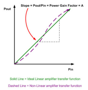
Figure 3.
An ideal linear amplifier, if one were to graph its output power versus input power, would have a perfectly straight line (See Figure #3) where the slope of the line would be the Power Gain Amplification Factor. This is simply a number that the input power is multiplied by to solve for the output power. Another characteristic of a linear transfer function is that the output frequency spectrum of the RFPAs output power is simply a larger amplitude replica of the input RF frequency spectrum.
Practical RFPAs are not perfectly linear (the non linearity arising from the non-linear transfer characteristics of the RF power transistors) and the Power Gain Amplification Factor is not a linear multiple but actually a complex transfer function with non-linear terms. Because of the non linear terms, There will be output frequency spectrums not only at in the input frequency spectrum but also at integer multiples (2, 3, 4n) of the input frequency. This is known formally as Harmonic Distortion or Harmonic Content. The bulk of the harmonic energy will be filtered out by the transmit coil, so low pass filtering of the RFPAs output is usually not required.
Specification (NMRS, MRIS): even order harmonics: -20 dbc, odd order harmonics: -12 dbc
5.2.4 Spurious RF output emissions (oscillation)
There are many forms of amplifier stability. Amplitude stability, for example, is a measure of the amplifiers ability to maintain a constant output level over long pulse sequence durations. A generic form of amplifier stability is its ability to maintain an output that is in some way controlled by the input. Spurious RF outputs are erratic frequency components that an RFPA puts out that can be either in its operational bandwidth or outside. The spurious output sometimes caused by inadequate filtering of output DC feed lines that couple RF signal power from the output of the RFPA to the input. They can be initially generated when an RF input is applied, yet can remain when the RF input is shut off. They are generally non harmonic related and can be close in or far away in frequency from the carrier. Wherever they are located, however, they are referenced in amplitude to the carrier frequency.
Specification (NMRS, MRIS) : < -50dbc
Another type of amplifier stability is Load-Pull stability. This is a measure of the amplifiers ability to maintain stable (or spurious-free spectral) operation while the output (or input) is subjected to various load impedances. Historically, amplifiers have been unrealistically specified as unconditionally stable for any magnitude/phase of source/load impedance.
The problem with an unconditionally stable requirement is that there is an infinite amount of source and load combinations to apply to an amplifiers terminals. In practicality, this simply cannot be verified.
In reality, the only true unconditionally stable two port network is a passive (Gain<1) network.
A more realistic way to specify and be able to verify amplifier stability is to define a load space on the Smith Chart and pick load Reflection Coefficients with discrete magnitude and phase values on which to test for spurious response.
For example, a specification for amplifier stability may read: Conditionally stable for up to 3:1 load VSWRs, rotational about the Smith Chart at 45 degree increments with less than -50 dbc of spurious frequency components.
5.2.5 Input VSWR (Input Return Loss)
Input Voltage Standing Wave Ratio or Input VSWR is measure of how close the input impedance of the amplifier is to an ideal 50 ohm resistor. The closer it is, the better it is matched to the RF signal source (assuming it has a 50 ohm output) and the better this match is, the more power will transfer from the pulse signal source to the RF amplifier. A 1:1 VSWR is a perfect match (i.e. all the power from the RF signal source will enter the RF amplifier). The higher the first number goes, the worse the impedance match is, and subsequently less power enters the RFPAs input.
Return loss is simply another way to express input match, only this is expressed as a logarithmic ratio of forward and reflected power.
Specification (NMRS, MRIS): Input VSWR: <2.0:1, Input Return Loss : <-9.5db
5.2.6 Output Noise (Blanked)
The NMR signal, be it from a patient or a sample is very faint. One way to improve Signal to Noise ratio is reduce all unnecessary electrical noise from the environment where the NMR signal is present. An RFPA generates quite a bit of noise while it is on as it has a large amount of Gain. The best way to reduce electrical noise out of an RFPA would be to simply shut it off. The problem with that is it takes far too long to turn the entire amplifier system on and off for it to be effectively used in an NMR/MRI system. The next best thing is only shut off the final stages of power amplification. This is accomplished by shutting off the bias to the output transistors as they can be switched on/off in under a microsecond. There will still be some noise output even with the output stage blanked off, to be certain, but the noise output now is tolerable.
Specification (NMRS, MRIS): -20db over thermal noise.
5.2.7 Noise Figure
A RFPAs job is to transmit sometimes very large amounts of RF power into a sample or patient. The magnitude of this RF energy is very large in comparison to the NMR signal. It may not seem essential for an RFPA to have a low noise output while it is transmitting since the very thing it is tasked to do is to generate RF power and lots of it. Why then would noise figure be important? The reason is that there are applications where the RFPA is transmitting at one frequency, however the RF receivers are listening at another and the lower Noise Figure an RFPA has, the less it will interfere with this second frequency.
Specification (NMRS, MRIS): <10 db
5.3 RFPA specifications, Power Domain
This is the last of the three Domains. In this area of specifications, the stimulus to be varied is power, that is, the input power to the RFPA is swept across a certain dynamic range (range of power levels, usually 30-40db). For example, if an RFPA is driven to full power at 0 dbm input, this unit would be tested with an input RF power level of -40 to 0 dbm. While the power is being varied, certain response parameters are being recorded such as Gain and Phase Linearity.
5.3.1 RF Power output
An RF Power Amplifiers output power capability is by far the first and foremost parameter that comes to mind when discussing an RFPA. How much power to use for a particular application in an NMR Spectrometer or MRI Scanner depends on many, many factors: coil (probe) limitations, SAR values, part of the anatomy to be scanned (i.e. head, extremities, and whole body) etc. It is truly beyond the scope of this discussion to quantitatively convey how to specify a maximum power output level for all applications. What can be discussed, however, is a rough estimate of what has been typically used to date. NMR RFPAs usually deposit their outputs into to some chemical sample, the size of the sample generally not large in volume. Most NMR applications run less than 500-2 kW of peak power up to 400MHz, from 400 MHz to 1 GHz, 100-500 Watts is adequate and from 1-2 GHz, 30-100 Watt amplifiers have been deployed.
MRIS RF power requirements can vary widely, as discussed. For extremities (arms, legs) in the 1- 3T realm 500-2kW is common, for head imaging, 4-8kW, and whole body amplifiers with up to 35 kW have been used. For higher fields (4, 7, 8, 9.4, 10.5 and eventually 11.7T) requests for power levels of up to 10-20kW are common. Multichannel 3T systems are running at 4kW per channel and multichannel 7T RFPAs are designed for 1kW per channel.
NQR applications have operated in the 2-4kW range and the far less common EPR experiments have be executed with anywhere from 400-2kW.
Although NMR and MRIS RFPAs are primarily used for pulsed applications, they are certain applications where they can be required to run in Continuous Wave (CW) mode. In this event, the required CW power is usually no more than 10% of the amplifiers maximum peak RF output power.
5.3.2 Gain Linearity
Pulse sequences can contain RF waveforms that have precisely proportioned amplitude ratios. An ideal linear amplifier has the unique characteristic that its output power is linearly proportional to the input power. Figure # 3 shows this graphically, which is a plot of output power vs. input power. The linear trace is called a transfer function, which describes the transfer relationship of input to output power of an amplifier.
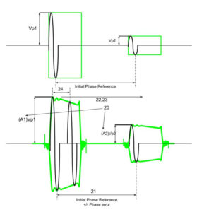
Figure 4.
The slope of the line is the power gain factor A, which (in an ideally linear amplifier; solid, straight plot) is some fixed, constant number regardless of what power level the output is. In actuality, the transfer function will not have a slope with a constant power gain factor, but one that is not linearly proportional to the input and will change over the dynamic range of the amplifier (dashed, curved plot). What this translates to is an amplifier that will amplify signals at low power one way, medium power another way and high power yet another way. By different ?ways? of amplification, it is meant that different power levels will be amplified by different power gain factors. This translates to a non linear gain transfer function. Figure # 4 shows how different amplitude pulses get different Power Gain Factors (A1 and A2).The Gain linearity specification quantifies how much deviation from ideal linear operation an actual amplifier can deviate from. In cases where the deviation from ideal is severe, the carefully proportioned amplitude ratios in a given pulse sequence can change dramatically.
The Gain linearity specification comes with a definition of dynamic range requirement as it must be understood and clarified, a priori, where the amplifier will be expected to be operated in terms of output power level. Usually the dynamic range is taken from the maximum specified output power level to some amount of db down from this level. The amount of dynamic range defined as a minimum should be 20 db, typically 40 db and in extreme performance applications 60 db.
Specification (NMRS, MRIS): Gain Linearity over 40 db dynamic range: +/- 1db of gain variation.
5.3.3 Phase Linearity
It takes a finite amount of time for a signal to make its way through an RFPA from its input connector to its output, and although it makes it through very fast (on the order of nanoseconds) there is a definite time expended. This delay time is called propagation delay and integral with this measurement is the parameter Insertion Phase. This is a measure of relative phase shift from the input to the output of the RFPA.? As with Gain Linearity, it would be preferred to have this relative phase shift to remain constant across the defined dynamic range of the RFPA. If the phase shift was constant then relative phase relationships between low power pulse signals and high power ones would be preserved throughout the amplification process. If the relative phase shift changes over the dynamic range, then the phase relationships are altered. This deviation is defined as Phase Linearity, and as with Gain Linearity, if comes paired with a defined dynamic range. The root cause of phase non-linearity is a parasitic junction capacitance present in all types of RF power transistors. This capacitance varies as a function of output power, so as the output power changes, so does this capacitance and along with it, the relative phase shift through the RFPA.
Specification (NMRS): Phase Linearity over 40 db dynamic range: +/- 5 degrees of insertion phase variation. Phase Linearity (MRIS): +/-7.5 degrees of insertion phase variation.
5.4 Safety specifications and System compatibility considerations (IEC-60601 and CE mark)
Up to this point, the primary focus has been the amplifiers performance relative to its ability to accurately reproduce an RF pulse sequence with an acceptable degree of fidelity. There are two other broad areas of amplifier specifications that worth covering in general so the end user or system engineer can be informed of their implications.
Safety is of primary importance with any electrical device, and RFPAs are certainly no exception. Specific Absorption Rate (SAR) is concerned with how much average RF power is deposited into a patient, one should be very clear on what the limitations are and have appropriate protection and limiting devices in place to automatically shut the RF amplifier off in the event SAR guidelines are exceeded. It is strongly recommended to have operationally redundant protection measures (i.e. independent, simultaneously operating average RF power monitoring devices) to limit RF power.
In addition to safety relative to the patient, safety concerns relative to the individuals who work with the RF power amplifier hardware are equally as important.
The safety protocol for both SAR and medical equipment is covered under the IEC-60601 safety standard. From the equipment perspective, an RFPA compliant to IEC-60601 will have undergone several months of independent safety tests performed on the unit. Organizations such as Underwriters Laboratories (UL) conduct thorough safety tests (including, but certainly not limited to) that verify the outer chassis is adequately grounded, wire insulation is appropriate for the voltage on a given conductor, circuit breakers and fuses are properly rated for deployment and that various, single point circuit failures will not present a hazard to the user. Perhaps most important, a unit that is marked as a UL recognized component, throughout the duration of that RFPAs manufacturing life cycle, the manufacturer will be subject to random audits to confirm the product is made conformant to the original UL approved design in terms of materials, components and also that the appropriate UL mandated production safety verification tests are conducted with test equipment that is calibrated and within its specified calibration cycle.
System Electro-Magnetic Compatibility (EMC) is covered by the CE Mark. The CE Mark is what the manufacturer applies to an RFPA after the unit has undergone and passed a battery of EMC tests. EMC tests are concerned with two major attributes of the RFPA; emissions and susceptibility. RFPAs generate a large amount of RF energy, the emissions aspect of EMC/CE testing measures the RFPAs ability to limit and contain its own radiated (RF energy emitted out of the RFPA chassis into its environment) and conducted (RF energy exiting the RFPA on interface and AC power cables connected to the unit) energy. This is a rough measure of how much a RFPAs operation may affect adjacent equipment.
The susceptibility portion of EMC/CE testing attempts to measure a RFPAs vulnerability to radiated (RF energy it receives from other equipment through the air) and conducted (RF energy it receives internally conducted through AC power lines and interface cables) energy.
In summary, the CE mark/EMC testing is a measure (however, by no means a guarantee) of how well an RFPA might perform in a given system environment. A unit that has a CE mark should be less likely to interfere with other equipments and conversely, its operation should be less impaired by other co-located noise generating electrical device, environmental disturbances (such as Electrostatic Discharge, ESD), lightning and AC power line surges and dips.
5.5 RFPA amplifier classes
RFPAs are designed to run in certain classes of operation. A class of operation loosely defines how the transistors in an RFPA amplify an RF pulse signal. Transistors operating in Class A amplify the full 360 degrees of the RF sinusoidal signal. Class A amplifiers are the most linear, most rugged (ability to tolerate bad loads), least efficient (<20%) and most expensive class of amplifier operation. Transistors operating in Class AB amplify slightly more than 180 degrees of the RF sinusoidal signal. Class AB offer a tradeoff of acceptable linearity reduced ruggedness, improved efficiency (approx 50%) and cost effectiveness. Class D/E amplifiers operate in switch mode (the transistors are switched on/off at the input RF frequency) are highly efficient (approximately 70%), yet extremely non-linear and require complex linearity error correction networks to make them usable for MRI.
